Low energy gamma detector – Rap47
Testing the new probe LEG (Low Energy Range) Kindly donated by George rap47 (GEO Electronics)
Rap47 – Documentation in PDF format
![]() LEG_Rap47_ITA
LEG_Rap47_ITA
![]() LEG_Rap47_ENG
LEG_Rap47_ENG
![]() LEG_Rap47_JAP
LEG_Rap47_JAP
![]()
![]() Rap47 –Editable documents in ODT format – Italian and English
Rap47 –Editable documents in ODT format – Italian and English
Those who know these languages could open the file in Open Office, fix them and send them to us. For other languages, you can take the file and have it translated to English: www.onlinedoctranslator.com/translator.html that is great, a breeze and respects the formatting.
LEG_Rap47_Documentation_ITA_ENG_JAP
Probe features RAP47
Type CsI (TL) (Cesium iodide doped thallium)
Dimensions Diameter 25.4 Crystal thickness 1.0 mm
Energy detected Range from 8 keV in 1 MeV.
Typical consumption 100% at 47keV, 80% to 100 Kev
Construction of the probe Anodized aluminium. Length 19 cm, diameter 3,8 cm.
Operating temperature from -25° C to 40° C
Operating humidity from 0 to 90%
Weight 178 g
Test Crystal scintillator NaI(TL) 24 X 40 mm former USSR
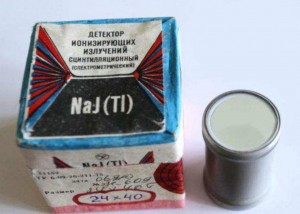
Alessio has tried these crystals and wrote a document with its characteristics. The pictures also illustrate well how to mount the Crystal in a probe over to look professional.
Russian_Scinillation_ITA
Russian_Scinillation_ENG
Cadmium Tungstate Crystal scintillator test (Cdwo4)
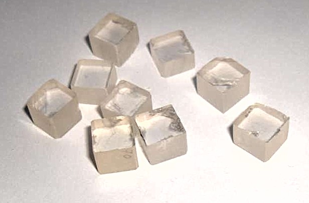
This type of Crystal is expensive and hard to find. It is also rather toxic, because of cadmium, and should be handled with gloves and mask, being for more very flaky. The probe ended, It is safe and non-hygroscopic.
The cadmium Tungstate is used mainly in places with strong radioactivity (> 10^ 4 Gray), but will endure long without damage. Has a very high density (7.9 GR/cm3) and a lower resolution than from NaI(TL), but better than that of BGO. The best resolution obtainable is around 8% (to 662 Kev).
The high density of this crystal makes it useful in making pocket sized probes, able however to detect high energy, even beyond the 2000 Kev. The light output is centered on 475 NM, suitable for coupling to a photodiode.
The decay time is very long compared to that of a Crystal NaI or CsI, the fact that sometimes leads to the need of hardware changes in FCM based on recognition of the shape. Using Theremino you can still also use this crystal, as you can see in the attached evidence.
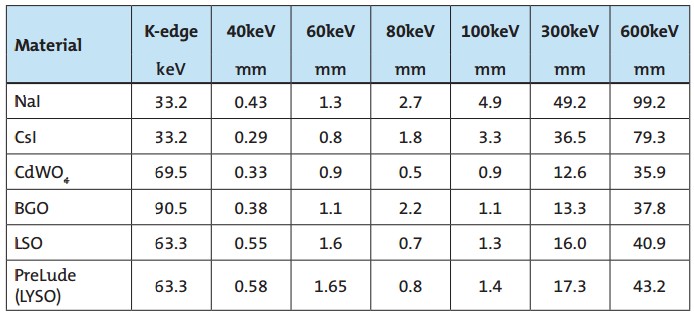
The Spectra produced by CdWO4 are lower than those of the NaI and the light output is only one third. But the CdWO4 can detect high energies, with a third of the thickness of the NaI. Basically you can save some tens of millimetres on probe length. The table below shows the most common thickness and energy characteristics of materials.
Measuring high voltages
To measure high voltages normal meters don't fit. Sometimes the scale of meters up to 1000 or 2000 Volts, but their impedance is too low.
Testers have an impedance from approximately 10 Mega Ohm, that would absorb the appliance under exaggerated power measurement 100 Milliwatts to 1000 Volts and up to a quarter of a Watt 1500 Volts. No high voltage generator makes sense (Apart from those used for executions) provides such powers. The ion Chambers and geiger tubes consume some uW (a hundred thousand times less) and the photomultiplier tubes (If wired right – with resistors 10 Mega) looking around 5 MW.
Why you should use a probe with very high impedance (at least 100 Mohm, but better if it is about 1 Gig Ohm).
– – – – – – – –
You can buy commercial probes but costing a great deal…
Don't buy these probes, contain only some resistor and don't have nothing special. You can build, with less than one Euro of components!
– – – – – – –
…or you can use complicated schemes with operational, protection diodes resistors and expensive 1 gig ohm, as the following:
Don't be tempted by patterns like this, need power supply (battery) and cannot measure negative voltages.
To measure a high negative voltage you would think to reverse the leads but we do not recommend that you do so, is not it nice to have the mass of the circuit and then also the operational and the trimmer adjustment for voltages of thousands of volts.
– – – – – – – – –
Simple version with traditional components
Instead, you should use a simple voltage divider with a series of resistors 10 Mega o 33 Mega totaling from 200 Mohm up to 800 Mohm and divide the voltage for 1000 with a calibration resistor in parallel to the tester.
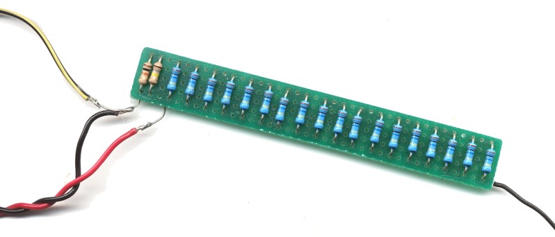
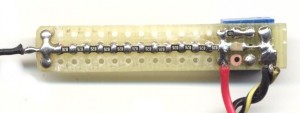
The red and black wires go to the tester, the yellow and black wire is the ground reference of high tension and the black wire to the right connects to high voltage.
The length of the resulting Strip makes very reliable this adapter even in humid conditions.
I recommend using a calibration resistor by one thousandth of the total resistance, with a low-value resistor in series, found by trial and error. Or you could use a resistor in series with a trimmer.
In this picture, the total resistance is 18 x 10 = 180 Mohm and calibration resistors are 180K + 10K
Calibration must be done on your tester. The resistance of some testers may be less than usual 10 Mohm. Better though if the tester is exactly 10 Mohm, the adjustment will be valid for use the adaptor with traditional probes 10 Oscilloscope mohm.
– – – – – – – – –
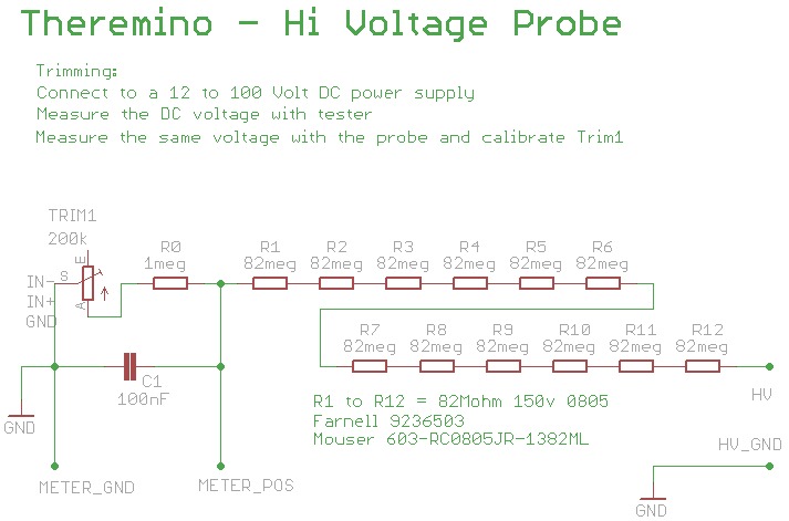
Theremino Hi Voltage Probe – SMD version from 1 Giga
With 12 resistors SMD, that cost in total 30 Euro cents, You can build a good probe from 1 Gig Ohm. The advantage of this version is to be able to stay in the container of a ballpoint pen.
The capacitor 100nF serves to stabilize the fit of the tenths of a Volt on the tester, even with long connecting wires and unshielded. To make measurements of signals that change over time (with oscilloscope) This capacitor decreases too much bandwidth and should be delete or disconnect from one side. To go from the probe to the oscilloscope using a shielded cable or very short.
Both the tester that the eventual scope should have an input impedance (input resistance) from 10 Mega Ohm. This is normal for all existing instruments but be careful not to use analogue meter may not work (You can calibrate the probe and would change by changing load tester)
When you connect an oscilloscope, it must be ensured that the probe is set to x 10. In this way its impedance is 10 Mega Ohm. If you set the scope probe x 1 its impedance becomes 1 Mega Ohms and it is no longer possible to calibrate the probe HV.
– – – – – – –
Theremino Hi Voltage Probe – Download
In this file the project Eagle PCB, the diagrams and pictures of all versions: Sensor_HvProbe
Minimize noise PmtAdapter
We assume that a lower power supply noise 1 MV pep creates disturbances in the area of energy under 2 Kev (that no sensor manages to reveal), and then you could accept it without problems.
But if someone wants to insist might find some new solution and give substantial help to all nit (like me among other things) they want to see the baseline absolutely flat and analysis with the DAA as clean as the following illustrations.
The terms of the problem
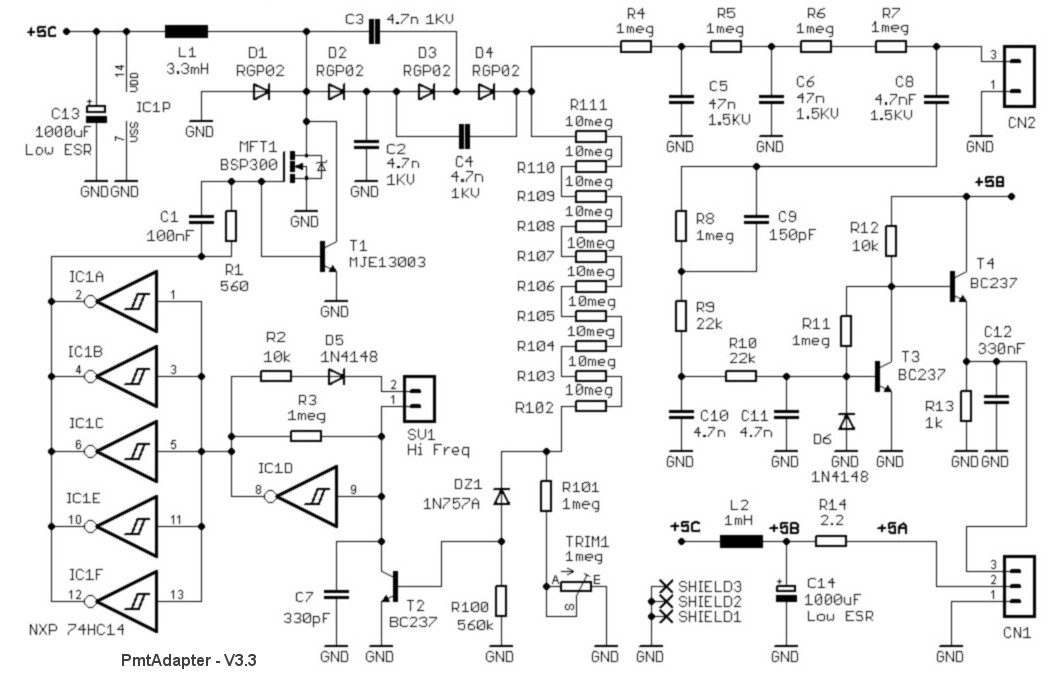
PmtAdapter scheme – Click the image for a larger view.
The mosfet and L1 are no impulses from 1000 Volts, and on the right side, PMT area, R8 and R9 and BNC would have reduced under 10 UV. Because 10 UV? Why would we want to stay under the 300 UV output, After T3 and T4, they earn about 20 times.
Between 1000 Volts and 10 There is a ratio of UV 100 million times and we are in the presence of pulses with steep faces, so high frequencies, passing through the minimum capacity thousandths of pF.
To make matters worse the PMT signal area is not necessarily high impedance (1 mega ohm) It also collects the ghosts, through the minimum capacity that exists through the air.
Going uphill the noise?
Looking at the diagram you can see that the left side (feeder) and the right side (signal) are joined only by four roads.
(1) The road R4, R5, R6: The two cells from 1 Mega + 47 NF are exaggerated and from there does not pass anything!
(2) The street L2 and R14: Here too, Thanks to the two 1000uF capacitors and the inductor from 1mH, the noise does not pass.
(3) Mass connections: Here begin the concerns, enough differences to increase noise from 300 UV pep to 1 MV pep
Ground loop short and Grand Chamber, that all would hold harmless, can create even dozens of mV of noise.
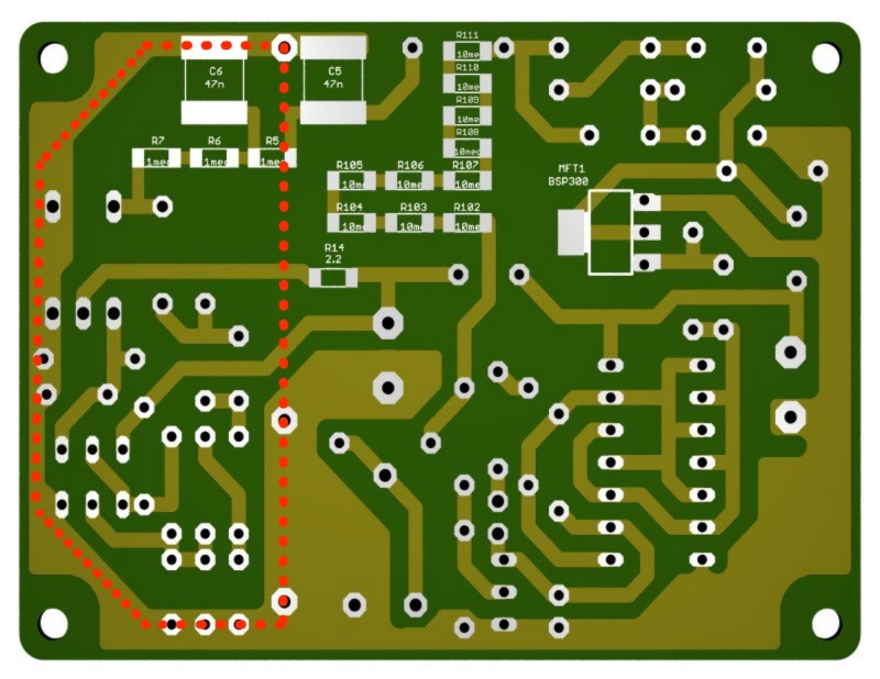
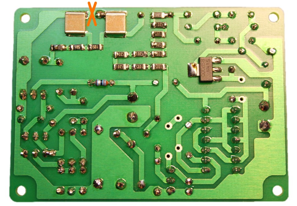
Check that the Ground-Loop of PCBs has been fixed with a cut at the point indicated by the Orange cross. (Click the images to enlarge them)
The first prototypes, with the PCB craft (get with the cutter), they behaved better and (under certain conditions of box, masses, sight unseen etc..) the disturbances came down under 300 uV pep.
The prototypes we used isolated BNC and the ground connection to the case was thoroughly in one place (through polo GND jack female), also used small boxes, just a few mm bigger than PCBS and only a trimmer for HV. So basically no wires in the box as shown in the next image.
With the big boxes, the connecting wires of the external potentiometer and the new machine made pcb, You cannot drop below to 500 UV pep and no one has yet found a solution. I get send four and even I couldn't remove the tacks on high frequencies and to fall under the 500 uV pep.
(4) The minimum capacity that bypasses the screen through the air: Here you can try many solutions, use a metal container smaller, in order to decrease the area on the sides of the screen, or enlarge the screen.
Don't neglect the two connection wires between the PCB and the BNC that should be short (less than 10 mm) and must be twisted between them. Very important even crush them down in order to bring them closer to the aluminum box base.
– – – – – –
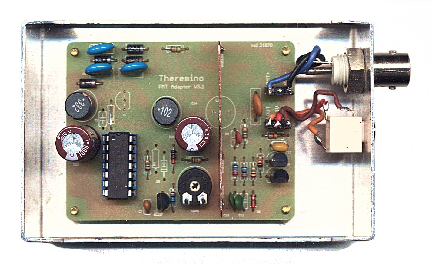
Those who want to cut to the Chase could attempt an exaggerated care (I recommend just to picky and that when I have time I'll try in person) it comes to halve the PCB and totally separate the two halves with a metallic screen that would divide the two halves of the housing.
The PCB should be divided exactly on the screen and you should reconnect R5 and R14 appropriately
Finally the two wires that go into the PSU should go into two small holes on the part.
We recommend this cutting operation only to those who have a lot of time and is very skilled in electronics. There are no certainties that it's worth it, No one has ever tried to do that, but most likely this may totally eliminate noise.
– – – – – –
Who will be able to find some simple and effective solution will be promoted super search-wizard-dott-prof Hunter of ailments and will have the gratitude of all of us!
Reduce the amplification of the Pmt Adapter
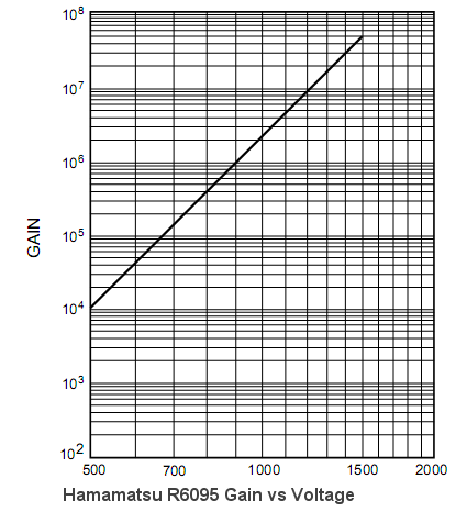
The Theremino PMT Adapter is designed, to give the best performance, with Hamamatsu photomultiplier R6095. Normally the R6095 and also other PMT, with similar characteristics, work well with “Audio gain = 2”, and a tension around 600..700 volts.
Some photo multipliers, eventually wired with resistor networks, other than the recommended (10 Mega on the dynodes and 1 Mega on the anode), can produce an output signal too high.
This condition is highlighted by the fact that you must keep “Audio gain” less than 2 and even the cursor “Energy trimmer” very low.
A signal too high, send in two Separate transistor saturation, worsens the linearity in the area of high energy and can, in the worst cases, completely masking the signals, of energy greater than a certain value.
The basic solution, to reduce the signal, is to reduce the supply voltage, the PMT.
One reads sometimes that PMT, have a fixed working voltage, but this is not true. All have a very wide adjustment range and PMT This serves to adjust their gain, Depending on your needs.
Lower the supply voltage has the beneficial effect of reducing the noise generated by PmtAdapter and reduce the risk of electrostatic, BNC connectors and capacitors.
If necessary, You can reduce the minimum voltage of PmtAdapter, even under the 500 Volts, replacing R101 with a resistor of highest value (for example, 1.8 Mega).
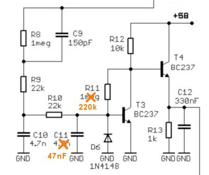
As a workaround, It can reduce the PmtAdapter gain.
The PmtAdapter gets bipolar pulse Gaussian and, using a delicate balance, the values of its components. So don't just adjust a single resistor.
This change reduces the gain to half, while preserving the characteristics of the pulses. Given that the gain has decreased, you will have to set the parameter “Audio gain = 2”, and readjust the tension on the PMT, in modo da lavorare con il cursore “Energy trimmer”, approssimativamente a metà.




Hello,
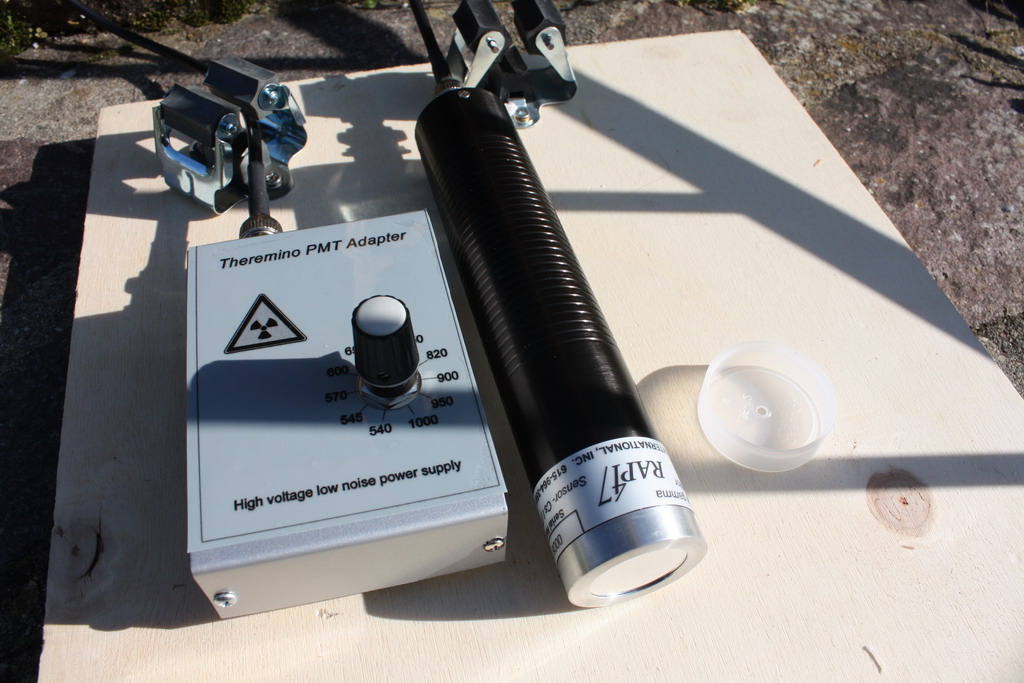
I’ve done some testing with Theremino PMT adapter, and I need some advice.
I used the same setting as the LEG_Rap47 document: https://www.theremino.com/wp-content/uploads/2013/03/LEG_Rap47_ENG.pdf
and finding some noise under 30 Kev.
It doesn’t bother so much if I cut off below 30kev, or so.
http://pico.dreamhosters.com/ThereminoPmtAdapter.html
I thought it’s because of USB power, and tried 2 different USB hubs. But I got about the same result.
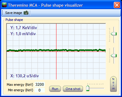
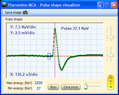
Here is the images of the test results with pulse analyzer showing noise pulse and normal pulse.
I reduced “max noise” to 5 (from 20) and “position” to 50 (from 80), and sometime “size” to 150 (from 300), to get results in tests this page:
http://pico.dreamhosters.com/ThereminoMcaSpectrums.html
What do you think I can do to reduce the noise at very low energy?
(I’ll try another computer that may have better USB power, later.)
I tried different volume level without visible changes.
I’ve put ferrite core on the audio cable without success.
Maybe where I live has too much EMF noise because I have many computers (although wifi and bluetooth are mostly off) or maybe because it’s rather high up (30 to 40m high) and getting radio signals from Digital TV station (2km away) and Cell stations (many of them all around).
If you have suggestion for baseline testing setting, cable or hardware solution (like using more ferrite core, etc) to try out, or any other ideas, please let me know.
Thank you
nkom
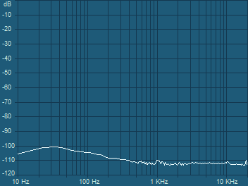
Your noise is about 500uV with a center frequency of about 10 kHz
With your settings a 500uV noise has the same height of 2 keV rows so it creates no problems.
But I have seen that you have a strong peak at about 10 keV that is produced by the ringing before the high energy pulses.
In your pulses of 11.3 keV and 11.5 keV you can see that the red vertical line is centered on the ringing that precedes the pulse.
Are you using the our USB cards modified with the internal HiPass filter ?
But the noise is not very high… try also to discover why there is so much ringing.
—————————————————————————
You noise is not produced from computers, wifi or bluetoots, it is completely generated by the audio card connections and ground loops. Ferrite can not correct this. Before all you must discover the noise path.
Try to move connectors, change cables and test:
– the audiocard alone,
– the audiocard + cable,
– the audiocard + cable + pmt adapter,
– the audiocard + cable + pmt adapter + PMT tube
Verify what is producing the noise
Try to make a better shield from the power supply and the preamp…
Do not connect ground wires – too much wires creates ground loops.
Do not use external power supply – only the usb 5V —>> audio card —>> PmtAdapter
—————————————————————————
I suggest to increase “Min. energy” to about 10 or 15 Kev
I think that there are not useful rows down 10 keV so this can be a good solution that will correct completely the problem.
Thank you fo suggestions.
The noise (measured with DAA) was like this:
Just sound card = 0.3mvpp 0.59 – 0.73mS
With sound cable = 0.3mVpp 0.59 – 0.71mS
With PMT adapter = 0.4 – 0.5mVpp 0.74 – 0.86mS
With BNC cable = 0.5mVpp 0.76 – 0.86mS
With Rap-47 = Hard to see, but it goes down to 0.5mVpp and then go up (with pulse, I suppose).
I’m not sure if the increse of 0.1 to 0.2mVpp when I connect PMT adapter is more than normal or not.
And there is only very slight increase with BNC cable.
——
I’ve done more testing with different HV setting (from 550kV to about 780kV),
and different sound level (from 2 to 30), as well as, Position, Size, and Max noise setting in the “Base line testing”.
And I could reduce the noise a lot with lower HV (about 650 or less), lower sound level (10 or less), smaller position like 50 (althout I’m not yet sure about this), higher Size of 300 instead of 240, and finally lower Max noise of 10 or less.
(The sound card is connected to USB hub that is powered by PC and without its own AC Adapter)
http://pico.dreamhosters.com/img/ThereminoMCA_2013_05_15_08_32_25-Rap47-BG-noise-correction.png
——
I did more testing with different setting.
It seems I can go down further in Max Noise, and other parameters.
Please see the tests I’ve done. (I did try lots of different setting)
http://pico.dreamhosters.com/ThereminoPmtAdapter.html
Your noise is OK, about 8 keV of amplitude ( 0.2 or 0.3 MV ) is normal and it is impossible to reduce it further.
I suggest to increase the “Min. energy” to about 10 or 15 keV in order to eliminate the noise from the left side of the graph. If not removed this noise can make the other rows disappear.
I have seen many pulses with the red line non in the pulse center – try to regulate the parameters to minimize the number of incorrect pulses.
But, in general your signals are OK, if you can not do better, maybe it is not possible.
A little percentual of “wrong” pulses is not a problem, if they are (for example) 1 every 100 good pulses, then the effect they produces is about invisible.
Good Job Alessio with your PMT adapter and Theremino MCA program !!!!
I test it today , I’m very happy to have a low cost gamma spectrometer !!!
Thank’s
Fabrizio
Thanks Fabrice,
you posted another time the same message, probably because it is not appeared in the page. This is because:
1) The english page is delayed by the translator (the italian page is updated immediately)
2) Messages without mail address are requiring a manual approvation.
Today we have changed the comment publishing rules and we hope that all the comments will appear immediately, also if the mail address is not specified.
Hello Livio , yes I have a little bug with my navigator !!!
I test it on another radioactive source.
Good program MCA !!!
Thank’s
Fabrice
Hello,
I do not know where elso to write a comment on your nice DAA application.
There is no other that useful than this.
Would it be possible to add an menue item to select the input device? It looks like the default one is chosen.
Also I cannot display spectra with Fmax more than 22kHz although input is at 192kHz.
Maybe you can do a revival of the DAA :-)
Regards,
Martin
Hi, Martin,
we have already planned to add a menu to select the input device.
Now we add to the todo list also to test if it is possible to increase the Fmax from 22 KHz to 100 KHz.
But this will require more investigations because probably all the audio cards have an hardware low pass filter at 22 KHz.
I do not know when we could do this, we have so many things to do…
(sorry for my bad english)
Hello Livio, It would need a HV probe up to 100kv DC and 10kv ac frequency from 35kHz and unfortunately the one presented on the site I think is not good… you can give me an advice? I saw that cost a lot… Thank you.
The probe we designed contains a dozen resistors 150 volts, so you can get about 2000 volts.
If there is no danger of drawing too much power from the circuit under test (and thus distorting measures) may be enough for three jig, and then three resistors in series (from 1 Giga and 10 KV), like this which costs 4 Euro:
https://www.mouser.it/ProductDetail/Ohmite/SM104031007FE?qs=sGAEpiMZZMttmiwpWlqA01XDd2CuKEml
If you can not too load the circuit under test you should use a dozen resistors 1 giga in series. All this would be a foot long, and unfortunately it would cost you quite a bit’ because those resistors cost 3.5 Euros each to take ten.
Or you could stretch to 100 or 120 resistors our project, would you take a while’ to solder them but it would be about 10 giga and very safe given the total length. This version will cost you fairly, SMD resistors of the series (from 82 Mega) Mouser, to buy cent, cost about 3.5 cents each, so spare, 3.5 Euros in total.
https://www.mouser.it/ProductDetail/Yageo/RC0805JR-0782ML?qs=sGAEpiMZZMukHu%252bjC5l7YWsW0TpwfWtXXbYA%2fKhRXRI%3d
Or (and I've done that) You could build a resistor along a thirty centimeters with the antistatic slats that contain integrated. It works but you have to practice with those who are up to establish the length and strength you are better. The biggest problem is to obtain a stable and lasting connection with the two terminal leads. I used the highly conductive black eraser, the I wrapped around the terminals and then wrapped there over many bare copper coils to tighten. After many years still they worked but they had changed a bit’ resistance. So if you spend much time (months or years) between a measurement and the following, must each time re-calibrate.
——–
In all cases the low side of the divider would be the same as that of our project, but without condenser if you want to see the high frequencies.
About the high voltage probes,
..any resistance has its own decoupling capacity expressed in volts than for smd regardless of their value in Ohm…it is very low!!!!
What you post? Something dangerous for others and for the equipment?
Many SMD resistors with the case 0805 or 1206 have an insulation capacity of 150 0 180 volts, go and see on any catalog, for example on Mouser. Then I guess it doesn't take you long to multiply by 12 and get about the 2000 that we have published.
Hello,
I’ve built two theremino MCA adapters for gamma sepectrometry and they work great when they do, however, at times the noise takes over and they stop showing data – only the tall column of noise. Normally it happens on the same day – as if something external affects them. May be humidity? I cannot figure it out.
I would be happy with any suggestions.
thank you!
Eugene
Hello Livio
Many months ago I find on Theremino page documentation about SiPM type MICROFC-xxx35-SMT with Eagle files for PCB for mounting this module (round platte). Unfortunately, now I can’t find this information.
Can you help me and give link for this information?
About at 40% of this page:
https://www.theremino.com/en/downloads/radioactivity
You find three lines saying:
SIPM – Solid State Photomultipliers
SiPM_ITA.pdf
SiPM_ENG.pdf
Thank you very much for your reply.
I know this project. It is unusefull for me.
I mean about this:
https://kitspace.org/boards/github.com/opengammaproject/microfc-sipm-carrier-board/
and Open Gamma Detector.
Many months ago I find very detailed description of this project, but after laptop data lose I haven’t more detailed information, but I have MICROFC-60035-SMT SiPM detector, PCB’s for it’s mounting and Open Gamma Detector hardware ver. 3.0.
I think, that the projects has been described also on Theremino. If not, excuse me.
Thank you
With best wishes
Andrew
The sensor cost about 50 on Mouser, then you need a NaiTl chrystal, a PCB and appropriate electronics, can you please estimate the total cost ?
I also know that the final sensitivity would be lower and the noise higher than what you get with photomultiplier tubes.
Perhaps the only advantage you might get with these SIPMs is to have a smaller probe. But the size doesn’t seem so important to me if in exchange the measurements lose quality.
Am I doing something wrong in these arguments?
Perhaps similar projects have been described on Physics Open Lab
https://physicsopenlab.org/category/english-posts/